
Product Images are shown for illustrative purposes only and may differ from the actual product.


 Store Pickup Available!
 Free Ship Over 5000 BDT
 Quality Product
 No Warranty
 No Replacement
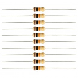
This pack of 10, 470Ω, 1/4W carbon film resistors allows you to stock up on a crucial component for your electronics projects. These resistors are ideal for a wide range of applications due to their standard power rating, compact size, and common tolerance level.
Each resistor features a through-hole design for convenient mounting on breadboards or permanent integration into printed circuit boards (PCBs). The color band coding on the resistors allows for easy identification of their resistance values. Featured By RoboticsBD.
Product Images are shown for illustrative purposes only and may differ from the actual product.
RoboticsBD RoboticsBD RoboticsBD RoboticsBD RoboticsBD RoboticsBD RoboticsBD RoboticsBD RoboticsBD RoboticsBD
RoboticsBD RoboticsBD RoboticsBD RoboticsBD RoboticsBD RoboticsBD RoboticsBD RoboticsBD RoboticsBD RoboticsBD
RoboticsBD RoboticsBD RoboticsBD RoboticsBD RoboticsBD RoboticsBD RoboticsBD RoboticsBD RoboticsBD RoboticsBD
| General Specifications | |
| Resistance Value | 470Ω |
| Power Rating | 1/4W (0.25W) |
| Tolerance | ±5% |
| Mounting Type | Through-Hole |
| Maximum Working Voltage | 300V |
| Maximum Overload Voltage | 600V |
| Operating Temperature Range | -55°C to +155°C |
| Quantity | 10 Pack |
| Shipment Weight | 0.005 kg |
| Shipment Dimensions | 3 x 3 x 3 cm |
Please allow 5% measuring deviation due to manual measurement.
RoboticsBD RoboticsBD RoboticsBD RoboticsBD RoboticsBD RoboticsBD RoboticsBD RoboticsBD RoboticsBD RoboticsBD
1 x 470 ohm 1/4w carbon Film Resistor - Pack of 10
RoboticsBD RoboticsBD RoboticsBD RoboticsBD RoboticsBD RoboticsBD RoboticsBD RoboticsBD RoboticsBD RoboticsBD
RoboticsBD RoboticsBD RoboticsBD RoboticsBD RoboticsBD RoboticsBD RoboticsBD RoboticsBD RoboticsBD RoboticsBD
The latest price of 470 ohm 1/4w carbon Film Resistor - Pack of 10 in Bangladesh is BDT 0 You can buy the 470 ohm 1/4w carbon Film Resistor - Pack of 10 at best price from our RoboticsBD or visit RoboticsBD Office.
|
Please note that the product information provided on our website may not be entirely accurate as it is collected from various sources on the web. While we strive to provide the most up-to-date information possible, we cannot guarantee its accuracy. We recommend that you always read the product labels, warnings, and directions before using any product. |
|
Product Images are shown for illustrative purposes only and may differ from the actual product. |
Reference: RBD-0846
Resistance: 27 kOhm Tolerance: 5% Max. Working Voltage: 250V Temperature Coefficient of Resistance: 50PPM/°C
Reference: RBD-0846
Resistance: 27 kOhm Tolerance: 5% Max. Working Voltage: 250V Temperature Coefficient of Resistance: 50PPM/°C