In stock

Call For Price
01783 007 004 Store Pickup Available!
 Free Ship Over 5000 BDT
 Quality Product
 No Warranty
 No Replacement
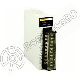
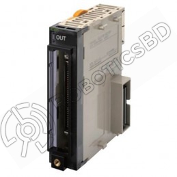
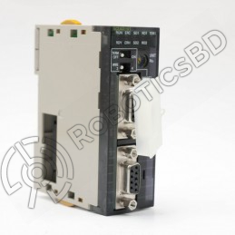
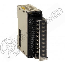
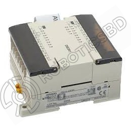
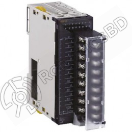
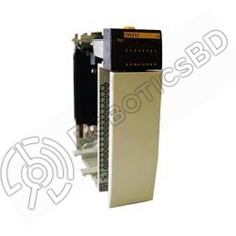
Omron CJ1W-OD262
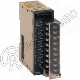
| Name | 8-point Contact Output Unit with Terminal Block (Independent Relays) |
|---|---|
| Model | CJ1W-OC201 |
| Max. Switching Capacity | 2 A 250 VAC (cosφ = 1), 2 A 250 VAC (cosφ = 0.4), 2 A 24 VDC (16 A/Unit) |
| Min. Switching Capacity | 1 mA 5 VDC |
| Relays | NY-24W-K-IE (Fujitsu Takamizawa Components, Ltd.), Cannot be replaced. |
| Service Life of Relay | Electrical: 150,000 operations (24 VDC, resistive load)/100,000 operations (240 VAC, cosφ = 0.4, inductive load) Mechanical: 20,000,000 operations Service life will vary depending on the connected load. |
| ON Response Time | 15 ms max. |
| OFF Response Time | 15 ms max. |
| Number of Circuits | 8 independent contacts |
| Insulation Resistance | 20 MΩ between external terminals and the GR terminal (500 VDC) |
| Dielectric Strength | 2,000 VAC between the external terminals and the GR terminal for 1 minute at a leakage current of 10 mA max. |
| Internal Current Consumption |
90 mA 5 VDC max. 48 mA 24 VDC max. (6 mA × No. of ON points) |
| Weight | 140 g max. |
| Circuit Configuration |
 The device variable names are the names that use "Jxx" as the device name. |
| External connection and terminal-device variable diagram |
 The device variable names are the names that use "Jxx" as the device name. The input power supply polarity can be connected in either direction. |
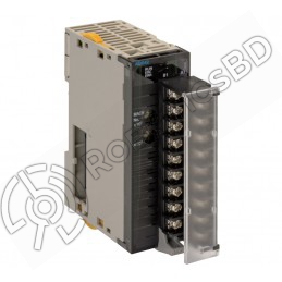
| Name | 16-point Contact Output Unit with Terminal Block |
|---|---|
| Model | CJ1W-OC211 |
| Max. Switching Capacity | 2 A 250 VAC (cosφ = 1), 2 A 250 VAC (cosφ = 0.4), 2 A 24 VDC (8 A/Unit) |
| Min. Switching Capacity | 1 mA 5 VDC |
| Relays | NY-24W-K-IE (Fujitsu Takamizawa Components, Ltd.), Cannot be replaced. |
| Service Life of Relay | Electrical: 150,000 operations (24 VDC, resistive load)/ 100,000 operations (250 VAC, cosφ = 0.4, inductive load) Mechanical: 20,000,000 operations Service life will vary depending on the connected load. |
| ON Response Time | 15 ms max. |
| OFF Response Time | 15 ms max. |
| Number of Circuits | 16 points/common, 1 circuit |
| Insulation Resistance | 20 MΩ between external terminals and the GR terminal (500 VDC) |
| Dielectric Strength | 2,000 VAC between the external terminals and the GR terminal for 1 minute at a leakage current of 10 mA max. |
| Internal Current Consumption |
110 mA 5 VDC max. 96 mA 24 VDC max. (6 mA × No. of ON points) |
| Weight | 170 g max. |
| Circuit Configuration |
 The device variable names are the names that use "Jxx" as the device name. |
| External connection and terminal-device variable diagram |
 The device variable names are the names that use "Jxx" as the device name. |
| Name | 8-point Triac Output Unit with Terminal Block |
|---|---|
| Model | CJ1W-OA201 |
| Max. Switching Capacity | 0.6 A 250 VAC, 50/60 Hz (2.4 A/Unit) |
| Max. Inrush Current | 15 A (pulse width: 10 ms max.) |
| Min. Switching Capacity | 50 mA 75 VAC |
| Leakage Current | 1.5 mA (200 VAC) max. |
| Residual Voltage | 1.6 VAC max. |
| ON Response Time | 1 ms max. |
| OFF Response Time | 1/2 of load frequency + 1 ms or less. |
| Number of Circuits | 8 (8 points/common, 1 circuit) |
| Surge Protector | C.R Absorber + Surge Absorber |
| Fuses | 5 A (1/common, 1 used) The fuse cannot be replaced by the user. |
| Insulation Resistance | 20 MΩ between the external terminals and the GR terminal (500 VDC) |
| Dielectric Strength | 2,000 VAC between the external terminals and the GR terminal for 1 minute at a leakage current of 10 mA max. |
| Internal Current Consumption | 220 mA max. |
| Weight | 150 g max. |
| Circuit Configuration |
 The device variable names are the names that use "Jxx" as the device name. |
| External connection and terminal-device variable diagram |
 The device variable names are the names that use "Jxx" as the device name. |
| Name | 8-point Transistor Output Unit with Terminal Block (Sinking Outputs) |
|---|---|
| Model | CJ1W-OD201 |
| Rated Voltage | 12 to 24 VDC |
| Operating Load Voltage Range | 10.2 to 26.4 VDC |
| Maximum Load Current | 2.0 A/point, 8.0 A/Unit |
| Maximum Inrush Current | 10 A/point, 10 ms max. |
| Leakage Current | 0.1 mA max. |
| Residual Voltage | 1.5 V max. |
| ON Response Time | 0.5 ms max. |
| OFF Response Time | 1.0 ms max. |
| Insulation Resistance | 20 MΩ between the external terminals and the GR terminal (100 VDC) |
| Dielectric Strength | 1,000 VAC between the external terminals and the GR terminal for 1 minute at a leakage current of 10 mA max. |
| Number of Circuits | 8 (4 points/common, 2 circuits) |
| Internal Current Consumption | 90 mA max. |
| Fuse | 6.3 A (1/common, 2 used) The fuse cannot be replaced by the user. |
| External Power Supply | 10.2 to 26.4 VDC, 10 mA min. |
| Weight | 110 g max. |
| Circuit Configuration |
 The device variable names are the names that use "Jxx" as the device name. |
| External connection and terminal-device variable diagram |
 load may operate incorrectly if the polarity is reversed. The signal names of the terminals are the device variable names. The device variable names are the names that use "Jxx" as the device name. |
| Name | 8-point Transistor Output Unit with Terminal Block (Sinking Outputs) |
|---|---|
| Model | CJ1W-OD203 |
| Rated Voltage | 12 to 24 VDC |
| Operating Load Voltage Range | 10.2 to 26.4 VDC |
| Maximum Load Current | 0.5 A/point, 4.0 A/Unit |
| Maximum Inrush Current | 4.0 A/point, 10 ms max. |
| Leakage Current | 0.1 mA max. |
| Residual Voltage | 1.5 V max. |
| ON Response Time | 0.1 ms max. |
| OFF Response Time | 0.8 ms max. |
| Insulation Resistance | 20 MΩ between the external terminals and the GR terminal (100 VDC) |
| Dielectric Strength | 1,000 VAC between the external terminals and the GR terminal for 1 minute at a leakage current of 10 mA max. |
| Number of Circuits | 8 (8 points/common, 1 circuit) |
| Internal Current Consumption | 100 mA max. |
| Fuse | None |
| External Power Supply | 10.2 to 26.4 VDC, 20 mA min. |
| Weight | 110 g max. |
| Circuit Configuration |
 The device variable names are the names that use "Jxx" as the device name. |
| External connection and terminal-device variable diagram |
 load may operate incorrectly if the polarity is reversed. The signal names of the terminals are the device variable names. The device variable names are the names that use "Jxx" as the device name. |
| Name | 16-point Transistor Output Unit with Terminal Block (Sinking Outputs) |
|---|---|
| Model | CJ1W-OD211 |
| Rated Voltage | 12 to 24 VDC |
| Operating Load Voltage Range | 10.2 to 26.4 VDC |
| Maximum Load Current | 0.5 A/point, 5.0 A/Unit |
| Maximum Inrush Current | 4.0 A/point, 10 ms max. |
| Leakage Current | 0.1 mA max. |
| Residual Voltage | 1.5 V max. |
| ON Response Time | 0.1 ms max. |
| OFF Response Time | 0.8 ms max. |
| Insulation Resistance | 20 MΩ between the external terminals and the GR terminal (100 VDC) |
| Dielectric Strength | 1,000 VAC between the external terminals and the GR terminal for 1 minute at a leakage current of 10 mA max. |
| Number of Circuits | 16 (16 points/common, 1 circuit) |
| Internal Current Consumption | 5 VDC 100 mA max. |
| Fuse | None |
| External Power Supply | 10.2 to 26.4 VDC, 20 mA min. |
| Weight | 110 g max. |
| Circuit Configuration |
 The device variable names are the names that use "Jxx" as the device name. |
| External connection and terminal-device variable diagram |
 load may operate incorrectly if the polarity is reversed. The signal names of the terminals are the device variable names. The device variable names are the names that use "Jxx" as the device name. |
| Name | 16-point Transistor Output Unit with Terminal Block (Sinking Outputs) |
|---|---|
| Model | CJ1W-OD213 |
| Rated Voltage | 24 VDC |
| Operating Load Voltage Range | 20.4 to 26.4 VDC |
| Maximum Load Current | 0.5 A/point, 5.0 A/Unit |
| Maximum Inrush Current | 4.0 A/point, 10 ms max. |
| Leakage Current | 0.1 mA max. |
| Residual Voltage | 1.5 V max. |
| ON Response Time | 15 μs max. |
| OFF Response Time | 80 μs max. |
| Insulation Resistance | 20 MΩ between the external terminals and the GR terminal (100 VDC) |
| Dielectric Strength | 1,000 VAC between the external terminals and the GR terminal for 1 minute at a leakage current of 10 mA max. |
| Number of Circuits | 16 (16 points/common, 1 circuit) |
| Internal Current Consumption | 5 VDC 150 mA max. |
| Fuse | None |
| External Power Supply | 20.4 to 26.4 VDC, 55 mA min. |
| Weight | 110 g max. |
| Circuit Configuration |
 The device variable names are the names that use "Jxx" as the device name. |
| External connection and terminal-device variable diagram |
 load may operate incorrectly if the polarity is reversed. The signal names of the terminals are the device variable names. The device variable names are the names that use "Jxx" as the device name. |
| Name | 32-point Transistor Output Unit with Fujitsu Connector (Sinking Outputs) |
|---|---|
| Model | CJ1W-OD231 |
| Rated Voltage | 12 to 24 VDC |
| Operating Load Voltage Range | 10.2 to 26.4 VDC |
| Maximum Load Current | 0.5 A/point, 2.0 A/common, 4.0 A/Unit |
| Maximum Inrush Current | 4.0 A/point, 10 ms max. |
| Leakage Current | 0.1 mA max. |
| Residual Voltage | 1.5 V max. |
| ON Response Time | 0.1 ms max. |
| OFF Response Time | 0.8 ms max. |
| Insulation Resistance | 20 MΩ between the external terminals and the GR terminal (100 VDC) |
| Dielectric Strength | 1,000 VAC between the external terminals and the GR terminal for 1 minute at a leakage current of 10 mA max. |
| Number of Circuits | 32 (16 points/common, 2 circuits) |
| Internal Current Consumption | 5 VDC 140 mA max. |
| Fuse | None |
| External Power Supply | 10.2 to 26.4 VDC, 30 mA min. |
| Weight | 70 g max. |
| Accessories | None |
| Circuit Configuration |
 The device variable names are the names that use "Jxx" as the device name. |
| External connection and terminal-device variable diagram |
 load may operate incorrectly if the polarity is reversed. Be sure to wire both terminals A9 and A19 (COM0). Be sure to wire both terminals B9 and B19 (COM1). Be sure to wire both terminals A10 and A20 (+V). Be sure to wire both terminals B10 and B20 (+V). The signal names of the terminals are the device variable names. The device variable names are the names that use "Jxx" as the device name. |
| Name | 32-point Transistor Output Unit with MIL Connector (Sinking Outputs) |
|---|---|
| Model | CJ1W-OD233 |
| Rated Voltage | 12 to 24 VDC |
| Operating Load Voltage Range | 10.2 to 26.4 VDC |
| Maximum Load Current | 0.5 A/point, 2 A/common, 4 A/Unit |
| Maximum Inrush Current | 4.0 A/point, 10 ms max. |
| Leakage Current | 0.1 mA max. |
| Residual Voltage | 1.5 V max. |
| ON Response Time | 0.1 ms max. |
| OFF Response Time | 0.8 ms max. |
| Insulation Resistance | 20 MΩ between the external terminals and the GR terminal (100 VDC) |
| Dielectric Strength | 1,000 VAC between the external terminals and the GR terminal for 1 minute at a leakage current of 10 mA max. |
| Number of Circuits | 32 (16 points/common, 2 circuits) |
| Internal Current Consumption | 140 mA max. |
| Fuse | None |
| External Power Supply | 10.2 to 26.4 VDC, 30 mA min. |
| Weight | 70 g max. |
| Circuit Configuration |
 The device variable names are the names that use "Jxx" as the device name. |
| External connection and terminal-device variable diagram |
 load may operate incorrectly if the polarity is reversed. Be sure to wire both terminals 23 and 24 (COM0). Be sure to wire both terminals 3 and 4 (COM1). Be sure to wire both terminals 21 and 22 (+V). Be sure to wire both terminals 1 and 2 (+V). The signal names of the terminals are the device variable names. The device variable names are the names that use "Jxx" as the device name. |
| Name | 32-point Transistor Output Unit with MIL Connector (Sinking Outputs) |
|---|---|
| Model | CJ1W-OD234 |
| Rated Voltage | 24 VDC |
| Operating Load Voltage Range | 20.4 to 26.4 VDC |
| Maximum Load Current | 0.5 A/point, 2 A/common, 4 A/Unit |
| Maximum Inrush Current | 4.0 A/point, 10 ms max. |
| Leakage Current | 0.1 mA max. |
| Residual Voltage | 1.5 V max. |
| ON Response Time | 15 μs max. |
| OFF Response Time | 80 μs max. |
| Insulation Resistance | 20 MΩ between the external terminals and the GR terminal (100 VDC) |
| Dielectric Strength | 1,000 VAC between the external terminals and the GR terminal for 1 minute at a leakage current of 10 mA max. |
| Number of Circuits | 32 (16 points/common, 2 circuits) |
| Internal Current Consumption | 220 mA max. |
| Fuse | None |
| External Power Supply | 20.4 to 26.4 VDC, 110 mA min. |
| Weight | 70 g max. |
| Circuit Configuration |
 The device variable names are the names that use "Jxx" as the device name. |
| External connection and terminal-device variable diagram |
 load may operate incorrectly if the polarity is reversed. Be sure to wire both terminals 23 and 24 (COM0). Be sure to wire both terminals 3 and 4 (COM1). Be sure to wire both terminals 21 and 22 (+V). Be sure to wire both terminals 1 and 2 (+V). The signal names of the terminals are the device variable names. The device variable names are the names that use "Jxx" as the device name. |
| Name | 64-point Transistor Output Unit with Fujitsu Connectors (Sinking Outputs) | |
|---|---|---|
| Model | CJ1W-OD261 | |
| Rated Voltage | 12 to 24 VDC | |
| Operating Load Voltage Range |
10.2 to 26.4 VDC | |
| Maximum Load Current |
0.3 A/point, 1.6 A/common, 6.4 A/Unit | |
| Maximum Inrush Current |
3.0 A/point, 10 ms max. | |
| Leakage Current | 0.1 mA max. | |
| Residual Voltage | 1.5 V max. | |
| ON Response Time |
0.5 ms max. | |
| OFF Response Time |
1.0 ms max. | |
| Insulation Resistance |
20 MΩ between the external terminals and the GR terminal (100 VDC) | |
| Dielectric Strength |
1,000 VAC between the external terminals and the GR terminal for 1 minute at a leakage current of 10 mA max. |
|
| Number of Circuits |
64 (16 points/common, 4 circuits) | |
| Internal Current Consumption |
5 VDC, 170 mA max. | |
| Fuse | None | |
| External Power Supply |
10.2 to 26.4 VDC, 50 mA min. | |
| Weight | 110 g max. | |
| Accessories | None | |
| Circuit Configuration |
 The device variable names are the names that use "Jxx" as the device name. |
|
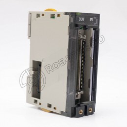
| External connection and terminal- device variable diagram | CN1 | CN2 |
 of the external power supply. The load may operate incorrectly if the polarity is reversed. Be sure to wire both terminals A9 and A19 (COM0) of CN1. Be sure to wire both terminals B9 and B19 (COM1) of CN1. Be sure to wire both terminals A10 and A20 (+V) of CN1. Be sure to wire both terminals B10 and B20 (+V) of CN1. The signal names of the terminals are the device variable names.The device variable names are the names that use "Jxx" as the device name. |
 of the external power supply. The load may operate incorrectly if the polarity is reversed. Be sure to wire both terminals A9 and A19 (COM2) of CN2. Be sure to wire both terminals B9 and B19 (COM3) of CN2. Be sure to wire both terminals A10 and A20 (+V) of CN2. Be sure to wire both terminals B10 and B20 (+V) of CN2. The signal names of the terminals are the device variable names.The device variable names are the names that use "Jxx" as the device name. |
|
| Name | 64-point Transistor Output Unit with MIL Connectors (Sinking Outputs) | |
|---|---|---|
| Model | CJ1W-OD263 | |
| Rated Voltage | 12 to 24 VDC | |
| Operating Load Voltage Range |
10.2 to 26.4 VDC | |
| Maximum Load Current |
0.3 A/point, 1.6 A/common, 6.4 A/Unit | |
| Maximum Inrush Current |
3.0 A/point, 10 ms max. | |
| Leakage Current | 0.1 mA max. | |
| Residual Voltage | 1.5 V max. | |
| ON Response Time |
0.5 ms max. | |
| OFF Response Time |
1.0 ms max. | |
| Insulation Resistance |
20 MΩ between the external terminals and the GR terminal (100 VDC) | |
| Dielectric Strength |
1,000 VAC between the external terminals and the GR terminal for 1 minute at a leakage current of 10 mA max. |
|
| Number of Circuits |
64 (16 points/common, 4 circuits) | |
| Internal Current Consumption |
170 mA max. | |
| Fuse | None | |
| External Power Supply |
10.2 to 26.4 VDC, 50 mA min. | |
| Weight | 110 g max. | |
| Circuit Configuration |
 The device variable names are the names that use "Jxx" as the device name. |
|
| External connection and terminal- device variable diagram | CN1 | CN2 |
 of the external power supply. The load may operate incorrectly if the polarity is reversed. Be sure to wire both terminals 23 and 24 (COM0) of CN1. Be sure to wire both terminals 3 and 4 (COM1) of CN1. Be sure to wire both terminals 21 and 22 (+V) of CN1. Be sure to wire both terminals 1 and 2 (+V) of CN1. The signal names of the terminals are the device variable names.The device variable names are the names that use "Jxx" as the device name. |
 of the external power supply. The load may operate incorrectly if the polarity is reversed. Be sure to wire both terminals 23 and 24 (COM2) of CN2. Be sure to wire both terminals 3 and 4 (COM3) of CN2. Be sure to wire both terminals 21 and 22 (+V) of CN2. Be sure to wire both terminals 1 and 2 (+V) of CN2. The signal names of the terminals are the device variable names.The device variable names are the names that use "Jxx" as the device name. |
|
| Name | 8-point Transistor Output Unit with Terminal Block (Sourcing Outputs) |
|---|---|
| Model | CJ1W-OD202 |
| Rated Voltage | 24 VDC |
| Operating Load Voltage Range |
20.4 to 26.4 VDC |
| Maximum Load Current | 2 A/point, 8 A/Unit |
| Leakage Current | 0.1 mA max. |
| Residual Voltage | 1.5 V max. |
| ON Response Time | 0.5 ms max. |
| OFF Response Time | 1.0 ms max. |
| Load Short-circuit Protection |
Detection current: 6 A min. Automatic restart after error clearance. |
| Line Disconnection Detection |
Detection current: 200 mA |
| Insulation Resistance | 20 MΩ between the external terminals and the GR terminal (100 VDC) |
| Dielectric Strength | 1,000 VAC between the external terminals and the GR terminal for 1 minute at a leakage current of 10 mA max. |
| Number of Circuits | 8 (4 points/common, 2 circuits) |
| Internal Current Consumption |
110 mA max. |
| Fuse | None |
| External Power Supply | 20.4 to 26.4 VDC, 50 mA min. |
| Weight | 120 g max. |
| Circuit Configuration |
 corresponding bit (two points per bit) in the Basic I/O Unit Information Area (A050 to A069) will change to TRUE. The signal names of the terminals are the device variable names. The device variable names are the names that use "Jxx" as the device name. |
| External connection and terminal-device variable diagram |
 may operate incorrectly if the polarity is reversed. The signal names of the terminals are the device variable names. The device variable names are the names that use "Jxx" as the device name. |
| Name | 8-point Transistor Output Unit with Terminal Block (Sourcing Outputs) |
|---|---|
| Model | CJ1W-OD204 |
| Rated Voltage | 24 VDC |
| Operating Load Voltage Range |
20.4 to 26.4 VDC |
| Maximum Load Current | 0.5 A/point, 4.0 A/Unit |
| Leakage Current | 0.1 mA max. |
| Residual Voltage | 1.5 V max. |
| ON Response Time | 0.5 ms max. |
| OFF Response Time | 1.0 ms max. |
| Load Short-circuit Protection |
Detection current: 0.7 to 2.5 A Automatic restart after error clearance. |
| Insulation Resistance | 20 MΩ between the external terminals and the GR terminal (100 VDC) |
| Dielectric Strength | 1,000 VAC between the external terminals and the GR terminal for 1 minute at a leakage current of 10 mA max. |
| Number of Circuits | 8 (8 points/common, 1 circuit) |
| Internal Current Consumption |
5 VDC, 100 mA max. |
| Fuse | None |
| External Power Supply | 20.4 to 26.4 VDC, 40 mA min. |
| Weight | 120 g max. |
| Circuit Configuration |
 Basic I/O Unit Information Area (A050 to A069) will change to TRUE. The signal names of the terminals are the device variable names. The device variable names are the names that use "Jxx" as the device name. |
| External connection and terminal-device variable diagram |
 may operate incorrectly if the polarity is reversed. The signal names of the terminals are the device variable names. The device variable names are the names that use "Jxx" as the device name. |
| Name | 16-point Transistor Output Unit with Terminal Block (Sourcing Outputs) |
|---|---|
| Model | CJ1W-OD212 |
| Rated Voltage | 24 VDC |
| Operating Load Voltage Range |
20.4 to 26.4 VDC |
| Maximum Load Current | 0.5 A/point, 5.0 A/Unit |
| Maximum Inrush Current | 0.1 mA max. |
| Leakage Current | 1.5 V max. |
| ON Response Time | 0.5 ms max. |
| OFF Response Time | 1.0 ms max. |
| Load Short-circuit Protection |
Detection current: 0.7 to 2.5 A Automatic restart after error clearance. |
| Insulation Resistance | 20 MΩ between the external terminals and the GR terminal (100 VDC) |
| Dielectric Strength | 1,000 VAC between the external terminals and the GR terminal for 1 minute at a leakage current of 10 mA max. |
| Number of Circuits | 16 (16 points/common, 1 circuit) |
| Internal Current Consumption |
5 VDC, 100 mA max. |
| External Power Supply | 20.4 to 26.4 VDC, 40 mA min. |
| Weight | 120 g max. |
| Circuit Configuration |
 Basic I/O Unit Information Area (A050 to A069) will change to TRUE. The signal names of the terminals are the device variable names. The device variable names are the names that use "Jxx" as the device name. |
| External connection and terminal-device variable diagram |
 operate incorrectly if the polarity is reversed. The signal names of the terminals are the device variable names. The device variable names are the names that use "Jxx" as the device name. |
| Name | 32-point Transistor Output Unit with MIL Connector (Sourcing Outputs) |
|---|---|
| Model | CJ1W-OD232 |
| Rated Voltage | 24 VDC |
| Operating Load Voltage Range |
20.4 to 26.4 VDC |
| Maximum Load Current | 0.5 A/point, 2.0 A/common, 4.0 A/Unit |
| Leakage Current | 0.1 mA max. |
| Residual Voltage | 1.5 V max. |
| ON Response Time | 0.5 ms max. |
| OFF Response Time | 1.0 ms max. |
| Load Short-circuit Protection |
Detection current: 0.7 to 2.5 A Automatic restart after error clearance. |
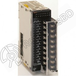
The latest price of Omron CJ1W-OD262 in Bangladesh is BDT 0 You can buy the Omron CJ1W-OD262 at best price from our RoboticsBD or visit RoboticsBD Office.
|
Please note that the product information provided on our website may not be entirely accurate as it is collected from various sources on the web. While we strive to provide the most up-to-date information possible, we cannot guarantee its accuracy. We recommend that you always read the product labels, warnings, and directions before using any product. |
|
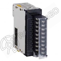
Product Images are shown for illustrative purposes only and may differ from the actual product. |
Call For Price
01783 007 004